Conductive Polymers for Advanced Electronics Manufacturing
Conductive polymers are transforming the future of advanced materials engineering, rapidly expanding from niche laboratory use into high-growth commercial applications such as flexible displays and circuits, printed electronics and conductive interconnects, energy storage devices, sensors, electromagnetic interference (EMI) shielding, and next-generation wearable devices. As industries demand lighter, more flexible, and highly functional materials, conductive polymers are emerging as a critical solution for next-generation product design and scalable manufacturing.
What are conductive polymers?
Conductive polymers are organic polymers that exhibit electrical conductivity while retaining the inherent advantages of plastics, including low weight, flexibility, and processability. Key conductive polymer systems, such as PEDOT:PSS (poly(3,4-ethylenedioxythiophene) polystyrene sulfonate), Polyaniline (PANI), and Polypyrrole (PPy), are gaining significant attention across industries due to their unique combination of electrical performance and manufacturability.
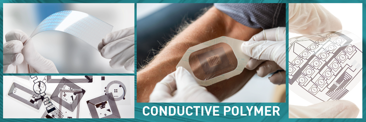
Conductive polymer materials enable a wide range of applications, including:
-
- Flexible, foldable, and curved displays
- Stretchable and wearable sensors
- Printed electronics, conductive interconnects, and smart packaging
- Wearable healthcare and biomedical monitoring devices
- Transparent conductive films for touchscreens and photovoltaics
- Antistatic and electrostatic discharge (ESD) coatings
Unlike traditional metal-based conductors such as copper or silver, conductive polymers can be processed using scalable, cost-effective methods, including coating, inkjet printing, screen printing, and roll-to-roll manufacturing. This compatibility with high-throughput production makes them especially attractive for emerging flexible electronics markets.
Key Manufacturing Challenges in Conductive Polymer Processing
Despite their advantages, conductive polymer formulations still present substantial processing challenges during development, scale-up, and high-volume manufacturing. Achieving consistent electrical performance while maintaining product quality requires precise process control, especially at the micro- and nanoscale.
Agglomeration and Non-Uniform Dispersion
Conductive polymer formulations often include complex mixtures of polymers, solvents, dopants, and functional additives. These components are prone to forming:
- Agglomerates and particle clusters
- Gel-like structures (micro-gels)
- Secondary particle networks
Without proper dispersion, these structures lead to non-uniformity in the final product, resulting in:
- Variations in electrical conductivity
- Poor coating uniformity and surface defects
- Reduced optical transparency in thin films
- Decreased mechanical strength and durability
- Inconsistent sensor and device performance
Achieving a uniform nanoscale dispersion is essential for ensuring reliable, high-performance conductive coatings, printed electronics, and conductive interconnects.
Limitations of Conventional Mixing Technologies
Traditional processing methods such as bead milling, rotor-stator mixing, or high-impact mechanical dispersion may not be suitable for sensitive conductive polymers. These techniques can introduce several critical issues:
- Polymer chain degradation
- Metal particle contamination
- Excessive heat generation
- Loss of conductivity
- Inconsistent particle size reduction
As conductive polymers are often used in high-value applications, such as medical devices, advanced electronics, and precision sensors, maintaining purity and structural integrity is paramount.
Advanced Solution: Star Burst Wet-Jet Milling Technology
Sugino’s Star Burst wet-jet milling system provides a highly advanced solution for overcoming the dispersion and homogenization challenges associated with conductive polymers. This innovative high-pressure technology enables superior processing performance without introducing contamination or thermal damage.
How Star Burst Technology Works
The Star Burst system uses ultra-high-pressure fluid-jet collisions and controlled shear forces to efficiently break down agglomerates and microgels. Unlike traditional milling approaches, this method achieves:
- Uniform nanoscale dispersion of conductive polymers and additives
- Effective breakdown of gel structures without damaging polymer chains
- Minimal heat generation during processing
- Contamination-free operation without grinding media
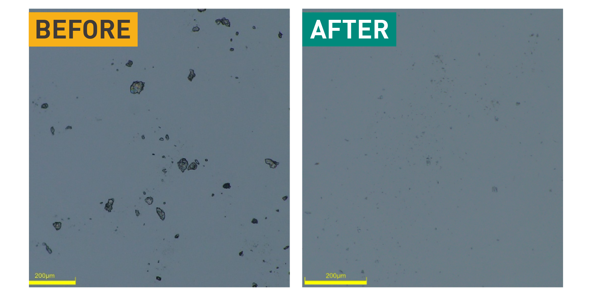
Before and After: Microscope Image of Star Burst Processing
Benefits for Conductive Polymer Applications
By integrating Star Burst homogenization into conductive polymer processing, manufacturers can achieve significant improvements in product quality and performance, including:
- Enhanced electrical conductivity consistency
- Improved coating smoothness and surface uniformity
- Superior transparency for optical applications
- Increased mechanical durability of films and coatings
- Reliable, repeatable performance in sensors and electronic devices
In high-performance applications, dispersion quality directly impacts the electrical, mechanical, and optical properties of the final product. Sugino’s advanced wet-jet milling technology ensures that conductive polymer formulations meet the demanding requirements of modern electronics manufacturing.
MORE TO READ:
Processing Raw Materials: Batteries
Processing Ceramics / Electronics Materials
Enabling the Future of Flexible Electronics
As the demand for flexible, lightweight, and high-performance electronic materials continues to grow, conductive polymers will play an increasingly critical role across industries. From wearable health-monitoring devices to next-generation energy systems, achieving precise dispersion and stable formulations is essential to unlocking their full potential.
Sugino’s Star Burst technology provides manufacturers with a powerful, scalable solution to overcome processing challenges and deliver consistent, high-quality conductive polymer products at an industrial scale.
Learn more about how Star Burst compares to conventional methods:

More to Explore
Watch processing videos for a range of materials

Learn how wet jet milling can improve and enhance your cosmetic and personal care formulations


